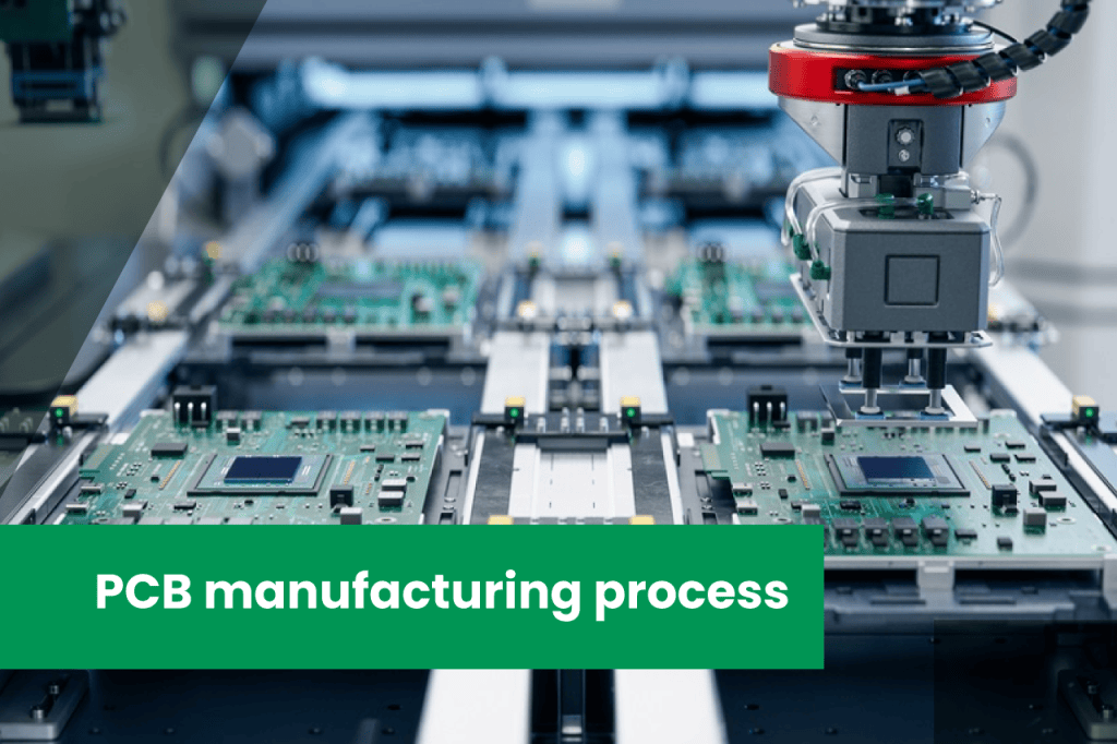
Printed Circuit Boards (PCBs) can be found at the centre of virtually every electronic device in our surroundings. PCBs quietly drive your technology, car, appliances, and medical devices, often without users understanding their significance. Manufacturing PCBs is both a modified and oftentimes complicated process of developing and engineering precision with meaningful design. Every detail is critical.
Before a final board reaches assembly, it has undergone several quality and technical steps which shape it, print it, drill it, and test it to perfect boards. Let’s now discuss in detail how a PCB comes to fruition.
PCB Manufacturing Process Steps
The PCB manufacturing process includes 16 core stages that take the idea from design to a ready-to-use board. These steps ensure that circuits are correctly aligned, layers are bonded securely, and electrical connections work flawlessly.
Step 1: Design and Output
Every PCB begins with a design. To create a detailed layout, engineers will use computer software like Altium Designer, Eagle, or KiCad. The digital blueprint consists of traces, holes, vias, and layers that make up the board.
Once the layout is approved, the design is prepared by PCB designers for export into Gerber files, which contain the position and information about the copper layers, solder mask, and silkscreen. These files serve as the manufacturing guide. Before production begins, engineers check them for errors through a process called Design for Manufacturability (DFM) review, ensuring everything fits real-world production limits.
Step 2: From File to Film
When the digital design is ready, it’s converted into physical films that act as templates for printing copper patterns on the PCB. Each layer of the board has its own film, one for copper routeing and another for solder masking.
A laser plotter prints the graphic images on clear plastic sheets. The dark areas indicate where the copper will remain, while the clear parts show what will be etched away later. This film is the visual reference for the next stages.
Step 3: Printing the Inner Layers — Where Will the Copper Go?
Now the actual board-making begins. The inner layers of the PCB start as a thin copper foil laminated on a dielectric material, often fibreglass (FR4).
A photoresist layer is applied to the copper surface, and the film from the previous step is placed on top. The board is then exposed to ultraviolet light. The light hardens the photoresist in the area where copper needs to remain. The areas that are protected by the dark parts of the film remain soft and will come off in the next step.
This step illustrates where the copper paths will carry electrical signals through the board.
Step 4: Removing the Unwanted Copper
The PCB is ready for the etch process. A chemical solution, often some sort of acid, removes the uncured copper from where it is not protected by the cured photoresist.
After etching, there remain the copper paths that will be the electrical connections in the circuit you built. Once etching occurs, the uncured photoresist is washed away, leaving the copper paths as part of the full electrical network.
This process requires accuracy because even a small over-etch can damage thin tracks or break circuit continuity.
Step 5: Layer Alignment and Optical Inspection
Multi-layer PCBs can be made with multiple inner copper layers; all of those layers have to have exact alignment prior to bonding. This is done in the optical punching step when optical punching machines can drill alignment holes through all layers using reference points from the design.
Following that will be an Automated Optical Inspection (AOI). The AOI machines equipped with cameras will scan each layer to see any defects like short circuits, over-etch, or missing traces. This is a time-efficient way to inspect using AOI; it allows the process to check each inner layer for quality and specifications before they are pressed together.
Step 6: Layer Up and Bond
After inner layers are inspected and ready, we can move on to building the full stack. The stack includes layers of copper and insulating prepreg sheets in the proper order. Each layer of copper is carefully aligned using pins for proper alignment in the stack to avoid a misaligned copper layer in the right combination.
When a proper stack is built, it will go into the lamination machine and be pressed with heat and pressure to fuse all layers into a solid board. When removed from the lamination machine, the copper and inner circuits are now fused in the internal structure of the board and ready for drilling.
Step 7: Drill
This will create holes for component leads and vias (the little copper-lined holes to connect layers). A CNC drilling machine will use coordinates from Gerber files to drill hundreds or possibly thousands of holes with very small drill bits.
Each hole’s size and location are critical, as they directly affect how components are soldered and how signals move between layers. After drilling, any debris or dust is cleaned using air jets or chemical washing.
Step 8: Plating and Copper Deposition
After drilling, the holes are empty and non-conductive. To make electrical connections between layers, the inner walls of these holes need a thin copper coating.
The board is subjected to the chemical plating process, where a very thin layer of copper is applied to each drilled hole in the substrate material, facilitating the flow of electrical signals from layer to layer. After chemical plating, the board goes through electroplating, which builds thickness on the copper (now solderable) and enhances conductivity and reliability.
Step 9: Outer Layer Imaging
When dealing with the outer layers of copper, the process is essentially the same. A new photoresist is applied, and the films are aligned to define the patterns for the top layer and the bottom layer circuits.
The photoresist is exposed to UV light so that the exposed photoresist hardens while the photoresist that was not exposed remains soft and removable.
Step 10: Plating
The exposed copper areas are thickened through electroplating. Additional copper builds up on the traces and inside the plated holes. At this stage, we may also add a thin layer of tin in preparation for the next step, to protect the copper that is underneath it, as we move into the etching process.
This reinforces surface copper and provides strong electrical pathways on the outer layers.
Step 11: Final Etching
The tin-covered copper is shielded while a chemical solution etches away the undesired copper. At this point, the tin is stripped away, revealing only the exact circuit patterns.
At this point, the inner and outer layers of the PCB have all been completed, making the whole conductive structure of the board.
Step 12: Solder Mask Application
The process results in the characteristic green (sometimes blue, red, or black) colour that all PCBs have. The solder mask is a thin layer of protective coating for the copper traces, serving to minimise oxidation and help to reduce solder bridging in the assembly process.
The board is coated with a liquid photoimageable solder mask and then exposed to UV light through a film that defines where the solder mask will remain and where it will be removed. The pads and holes where components are to be soldered will be exposed.
After etching, the board is baked, which cures the solder mask, ensuring durability and thermal resistance.
Step 13: Surface Finish
Bare copper oxidises rapidly in open situations, so a surface finish is applied that protects copper and allows good solderability. Various surface finishes are used as required for their designated product; these include HASL (Hot Air Solder Levelling), ENIG (Electroless Nickel Immersion Gold), OSP (Organic Solderability Preservative), and ENEPIG (Electroless Nickel Immersion Gold with Palladium).
Each of these finish types offers their own trade-off of cost, performance, and durability. For instance, ENIG gives a smooth, flat surface and is ideal for fine-pitch components, while HASL is more cost-effective for general use.
Step 14: Silkscreen
Next, the silkscreen layer is printed. The layer contains text, symbols, and markings for components that will help engineers identify parts of the board and test-points.
The white ink is used more often than not and the markings are applied either by screen printing or by the inkjet process. In addition to being important for assembly, the silkscreen is also important during the maintenance and debugging aspects of the process.
Step 15: Electrical Test
A PCB assembly cannot progress to the assembly process until it has been verified to ensure all circuits are correctly connected with no shorts or open circuits.
Automated machines use a flying probe or bed-of-nails tester to check continuity across every net on the board. This ensures that the board will operate as intended per the design file.
A PCB that passes the verification test is considered electrically sound and can be moved into the final shaping process.
Step 16: Profiling and V-Scoring
To finish, the PCBs will be removed from the production panel. Routeing machines or V-scoring tools will create the desired shape of the board as well as provide the edges.
V-scoring makes it easier to remove PCBs once produced by creating small scores in between boards to simplify breaking out. Once the profiling is done, the boards are cleaned and prepared for packaging.
Conclusion
Overall PCB manufacturing is an art and an engineering exercise in balance. Each step taken in the process following design will allow the manufacturer to create a PCB that is reliable, accurate, and ready to be integrated into modern electronics.
The PCBs that you will couple with hours of careful design capabilities with machines and the skilful eyes of humans to monitor. The result is a compact piece of technology that carries the power of innovation in every trace and via.
At Elemental Electronics, we bring high-tech and innovative design solutions to businesses and organisations that want to create modern technology products. Our Electronics Designers utilise the latest in design technology to transform concepts into physical and software-driven products and solutions. Almost all our clients opt for our turnkey approach, where the design, validation, and manufacturing of their products are all handled in-house by our expert team.