We live in a world that runs on electronics. Every gadget you use, from your phone to your coffee maker, has layers of circuitry hidden inside. Printed circuit boards are the backbone of those devices. But here is the real issue. The way we make and throw away electronics leaves a big mark on the planet.
We make more and more gadgets every year. That means more waste. The planet handles this poorly. The environmental impact of electronics is now huge. Millions of tons of e-waste are thrown out annually.
In 2022 alone, around 62 million tonnes of electronic waste were produced worldwide, yet only 22.3 percent were recycled in a proper way.
That stat should make anyone stop and pause. We have valuable materials in these gadgets, but they are lost when circuits end up in landfills or informal recycling sites.
PCB manufacturers are now working on new eco-friendly PCB technology like 3D-printed PCBs and recyclable PCBs. These innovations could change the way we make and recycle electronics.
In this blog we look at what these sustainable solutions are and why they matter.
Why does sustainability in electronics matter?
You might hear the term “sustainability” everywhere now, but in electronics it means using less energy, fewer toxic materials, and designs that can be reused or recycled easily. Electronics manufacturing has historically been very linear. We take materials from earth, make products, sell them, and then throw them away. This path increases resource depletion and pollution, just piling up waste.
Electronic devices contain metals like gold, silver, copper, and rare earth elements. These are limited resources. Mining for them takes a huge environmental toll. Worse, many of these metals end up wasted in landfills.
The electronics industry contributes to some 2–3 percent of global greenhouse gas emissions, and these emissions are linked to energy for making and transporting parts.
One big reason this matters is e-waste. It is one of the fastest-growing types of waste we make. Electronics break or fall out of favor so quickly that entire mountains of circuits are discarded. Sometimes they are burned in open sites with little protection, which releases toxins into air, soil, and water.
Rise of e-waste → need for recyclable, low-impact PCB solutions
Data shows the amount of e-waste we generate keeps rising fast. Between 2010 and 2022, global e-waste went up sharply. This trend is expected to continue. In fact, by 2030 we could be creating around 82 million tonnes of e-waste every year if things stay the same.
This makes it clear we need better ways to handle circuits. Traditional PCBs are difficult to recycle because they are made with materials that do not break down easily. Plastic, fiberglass, copper, and solder all fused together. That is where recyclable PCBs and new production methods like 3D-printed PCBs step in.
What Are 3D-Printed PCBs?
3D-printed PCBs are exactly what they sound like. Instead of the usual layered fabrication, electronics are printed layer by layer. This can be done with different materials for conductors and substrates. Sometimes it is plastic that dissolves or separates easily; sometimes it is water-soluble material that leaves behind a clean board. These types of boards are much easier to take apart and recycle.
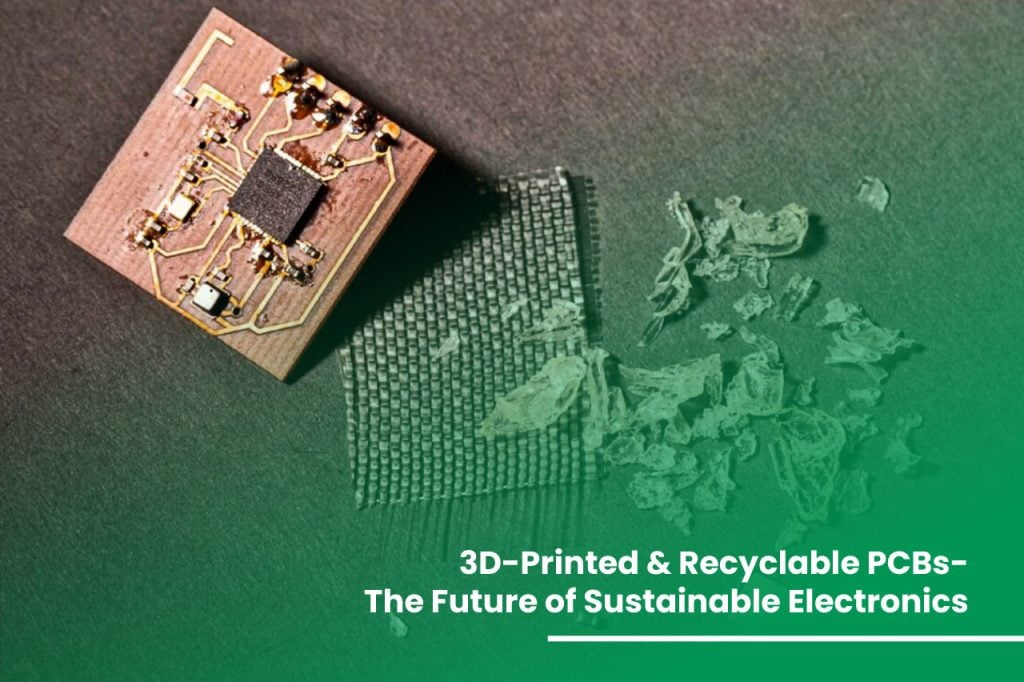
One exciting development in this space is a board made with PVA-based PCBs and liquid metal circuits. When placed in water, the board dissolves and separates, letting you recover both the board and the metal. This means nearly all materials can be reused again and again, unlike traditional PCBs.
Rise of Recyclable & Dissolvable PCB Materials
Recyclable and dissolvable materials are gaining attention because they fit well with circular electronics manufacturing. The concept of circular manufacturing strives to keep materials in use for as long as possible rather than dumping them into the environment.
Materials like water-soluble PVA and other green PCB materials help reimagine circuits. Engineers are exploring these for prototyping and even more permanent solutions. What’s fun here is that the board can be designed to break apart easily at the end of life. That changes how we think about waste. Instead of trash, it becomes a resource.
This trend toward sustainable electronics PCBs is not just about novelty. It is a response to the real weight of e-waste on our planet. And it points to a future where parts are reused, melted down, or repurposed rather than landfilled.
Key Benefits of 3D-Printed & Recyclable PCBs
Lower environmental footprint
Sustainable PCBs reduce the total energy used to produce and dispose of circuits. They avoid harsh chemicals and toxic waste, which helps cut pollution from the manufacturing line all the way to the recycling bin.
Better material recovery
Since recyclable PCBs can be disassembled with water or other simple procedures, precious materials such as copper and precious metals can be reutilized, therefore saving mining and reducing the environmental devastation defined with resource extraction.
Faster prototyping and flexibility
3D printing also allows for rapid design and manufacturing of boards. It also facilitates engineers in carrying out tests on their designs faster with no need to produce piles of failed prototypes. The boards consume less material that is difficult to recycle.
Support for circular electronics manufacturing
These boards fit into a system where products are built to be reused and recycled, not thrown away. That is a core idea behind eco-friendly PCB technology and circular manufacturing.
Applications of Sustainable 3D-Printed PCBs
Prototyping and research labs
Designers can quickly print boards for testing without worrying about waste at the end of a project.
Educational makerspaces
Students and hobbyists can learn electronics in such a way that it allows the reuse of material rather than generating trash.
Wearable tech and short-life-cycle devices
Shorter life cycles of products stand to significantly benefit from recyclable PCBs, as many parts can be recovered easily.
Low-volume specialty electronics
In cases where custom boards are required, 3D printing with recyclable materials can reduce waste and expense.
Challenges & Limitations
Material performance limits
Though such removable materials exist, they may, nonetheless, not be exactly on the same footing with respect to durability/dependability when it comes to common PCB materials.
Scaling production
There is still a need for innovation in mass printing and recycling.
Cost concerns
New materials and equipment may also be quite costly.
Industry standards and adoption
Big firms may take time to transform. Standards for recyclable electronics PCBs are still evolving.
The Future: Fully Recyclable Electronics?
Here is where things get interesting. Today’s sustainable PCB technology is just the beginning. Materials like PVA-based PCBs and liquid metal circuits show that we can recover almost all parts of a circuit board at the end of its life. That fits well with a circular economy. In a true circular system, nothing is wasted; everything is reused either as a new board, a new device, or another product.
A future where electronics do not end up in huge toxic mounds feels possible. It will take cooperative efforts from electronic manufacturers, policymakers, and consumers. Better design, better materials, and smarter recycling infrastructure will all play a role.
We may also see more green PCB materials that are entirely harmless to the environment and adopt regulations that make recycling mandatory or easier for companies around the world.
Conclusion
The growth of electronics shows no signs of slowing down. This is why a greater need for environmentally sustainable electronics PCBs, which have the ability to be recycled/reused, exists. We recognize that 3D Printed PCBs, as well as Recyclable PCBs, are a part of this solution. They help minimize waste and recover valuables, while even opening up new ways of making and using electronics.
By supporting innovation in this space and pushing for eco-friendly PCB technology, we can help divert electronics from a linear waste path into a circular one. And the planet, together with the future generations, would thank us for that.